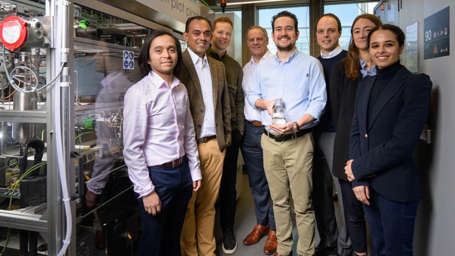
UC Berkeley’s Marvell NanoLab gets high-tech boost with Lam Research gift

Sophisticated etching system enables atomic-scale precision for next-generation chips
April 16, 2025
Researchers at UC Berkeley Engineering will soon have access to a multimillion-dollar semiconductor manufacturing system that will enable the fabrication of nanoscale semiconductor devices for next-generation chip technologies. Lam Research, headquartered in Fremont, Calif., has donated an innovative multi-chamber etching system to the Berkeley Marvell Nanofabrication Laboratory at CITRIS.
“We thank Lam Research for its many contributions over the years to UC Berkeley’s Marvell NanoLab in support of research and innovation for nanofabrication technologies,” said Tsu-Jae King Liu, dean of UC Berkeley’s College of Engineering. “Lam’s latest donation gives our researchers and students access to wafer-processing capabilities rarely accessible outside of the most sophisticated semiconductor manufacturing facilities. I look forward to seeing Lam’s advanced etching system enable new atomic-scale process innovations
To continue the advancement of Moore’s Law, which posits that the number of transistors on a microchip doubles approximately every two years, ever-tinier components are needed. Michael Helmbrecht, executive director of the Marvell NanoLab, said the new semiconductor etching system has the level of precision needed to manufacture the nanoscale components needed for such advanced systems.
“This semiconductor etching system allows us to remove material from wafers, one atom, one molecule at a time,” he said. “This is especially important as we design and manufacture nanometer-scale transistors.”
This latest upgrade continues UC Berkeley’s history of innovation in transistor fabrication, a tradition that dates back to the 1962 launch of the Integrated Circuits Laboratory, considered the first university-based laboratory of its kind in the world. Capabilities of the lab were continually enhanced to meet the requirements of more advanced circuit processing. The IC Lab was upgraded to the Microfabrication Laboratory in 1983 and succeeded by the Marvell NanoLab in 2010.
The Marvell NanoLab serves 350 researchers from multiple campuses and national research laboratories, including Lawrence Berkeley National Laboratory, UCSF and Stanford University. More than two dozen industrial companies also use the facility.
“Very few, if any, university labs other than UC Berkeley have anything like this capability,” said NanoLab faculty director Kris Pister, professor of electrical engineering and computer sciences. “Researchers here will be able to develop new integrated circuit device technologies that improve the performance of everything from cell phones to AI to quantum computing hardware.”
See related
link


